Decoupling Capacitor Placement: Simulation vs Bench Reality on a 4-Layer Board
SPICE says your decoupling works. The spectrum analyzer says otherwise. A board that taught me why placement matters more than value above 100 MHz.
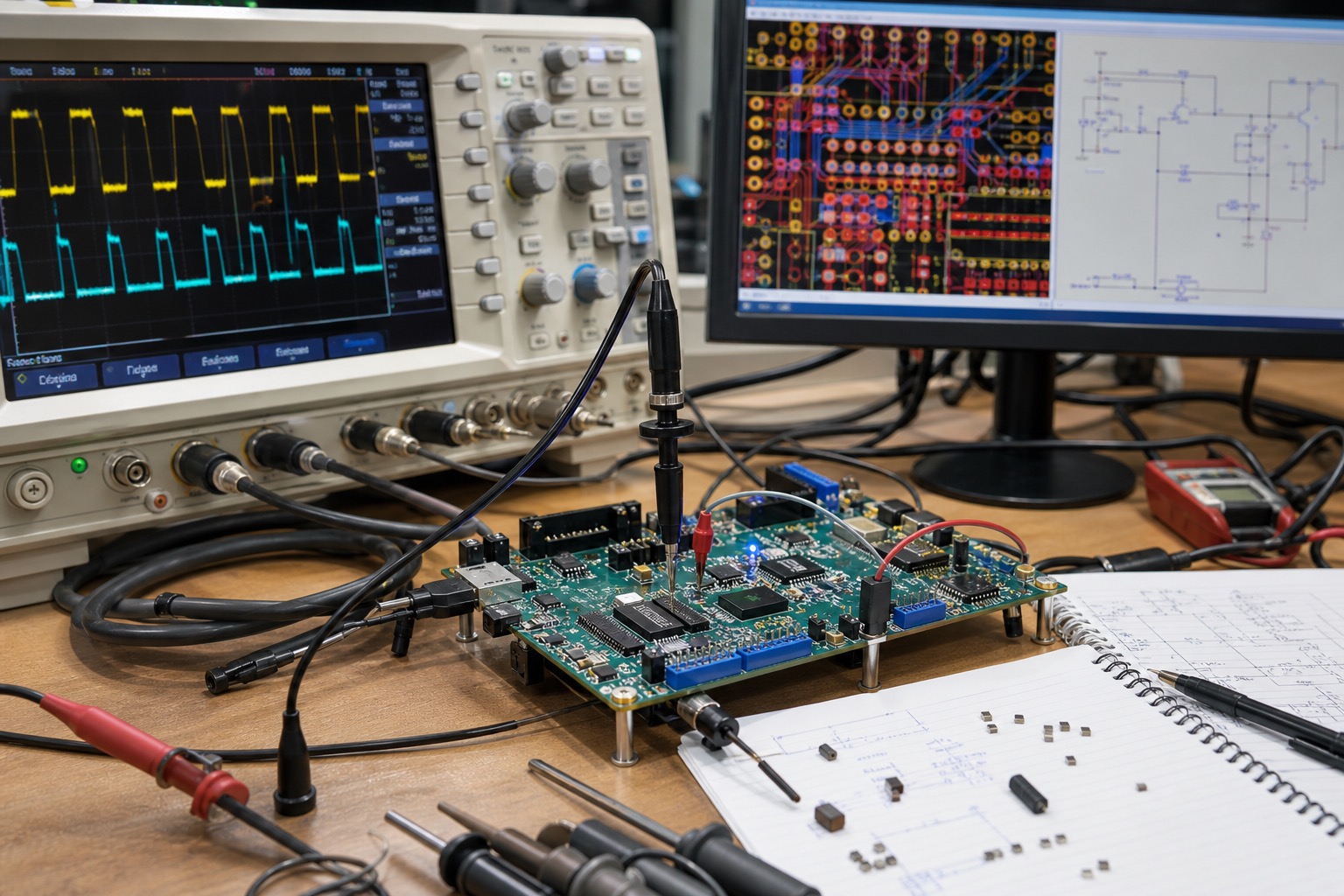
SPICE said the 100 nF caps on my STM32F407 board were fine. A Rigol DSA815 spectrum analyzer said the 168 MHz clock harmonic was 12 dB over the Class B pre-compliance limit at 3 meters equivalent. The fix was not more capacitance — it was 6 mm less distance between LQFP power pins and the correct cap.
Lab note from a 4-layer board (Sig/Gnd/Pwr/Sig), 1.6 mm FR-4, KiCad 7 layout that taught me decoupling above 100 MHz.
Board context
- MCU: STM32F407VGT6, LQFP-100, running at 168 MHz from 8 MHz HSE + PLL
- Decoupling per ST AN4488: 100 nF per VDD/VSS pair + 4.7 µF bulk per power group
- Problem frequency: 336 MHz (2nd harmonic) and 504 MHz (3rd) radiating via power rail impedance
Initial layout: caps placed in a row near board edge "for cleanliness." Electrically connected. Physically too far.
SPICE vs reality gap
What simulation assumed
Ideal ground plane, zero inductance vias, cap ESL = 0.5 nH (0402 nominal). AC sweep showed impedance < 0.1 Ω up to 200 MHz at VDD pin.
Tool: LTspice XXVII, Murata SimSurfing S-parameter models for GRM155R71C104KA88D (100 nF 0402 X7R).
What bench measured
VDD pin impedance (Picotest J2102A injector + Bode 100A):
| Frequency | SPICE | Measured |
|---|---|---|
| 50 MHz | 0.08 Ω | 0.31 Ω |
| 168 MHz | 0.12 Ω | 1.8 Ω |
| 336 MHz | 0.15 Ω | 4.2 Ω |
Measured peak at ~380 MHz — self-resonance of cap + loop inductance, not in SPICE because layout loop wasn't modeled.
Loop area: cap on bottom layer, via to plane, trace to VDD pin — 8.4 mm path vs recommended < 2 mm from pin.
What actually fixed EMC
Placement priority (ordered)
- 100 nF on every VDD pin pair — literally the two pins closest to the cap on same layer as MCU when possible
- Via to ground plane adjacent to cap ground pad — twin vias for 0402 when space allows
- 4.7 µF bulk within 5 mm of power entry to MCU group, not near crystal
- Do not share vias between digital and analog decoupling networks on STM32 VDDA
Moved caps from board edge to hugging pins 12/13, 24/25, etc. Rework on 10 boards — hot air, same BOM.
Result: 336 MHz harmonic down 14 dB. Passed pre-compliance with 3 dB margin.
Value mattered less than placement above 100 MHz
Swapped 100 nF → 47 nF → 22 nF at same bad placement: < 2 dB change at problem harmonic.
Same 100 nF at good placement: 14 dB improvement.
Below ~50 MHz, bulk cap value and placement toward power entry mattered more — different failure mode (brownout on LDO step), different fix.
4-layer stackup constraints
Power plane split (3.3 V digital / 3.3 V analog) increased return path length for digital caps. AN4488 recommends keeping VDDA isolated; we learned:
- Ferrite bead on VDDA (BLM18PG121SN1D) helped analog ADC noise but didn't fix digital harmonic radiation
- Stitching vias every 5 mm along split boundary reduced return path for digital currents
See EMI bench testing notes for full scan setup — same DSA815, near-field probe for localization before chamber time.
Power sequencing interaction
Decoupling insufficient during power-up ramp caused different symptom — MCU brown-out reset. Related to power sequencing design: bulk cap too far delayed local energy delivery during LDO enable edge.
KiCad-specific lesson
DRC doesn't know frequency. Added custom rule: decoupling within 2 mm of VDD pin — manual review checklist until KiCad 8 constraint regions mature.
Part selection nuance
We tested 0402 vs 0201 100 nF caps at correct placement — 0402 won on EMC (lower ESL in Murata models) but 0201 was acceptable within 1 dB if placement perfect. Assembly rework favor 0402 for hand solder on prototypes.
X7R vs C0G above HF: C0G 100 nF too large physically; X7R DC bias derating matters — 3.3 V rail on 6.3 V rated cap loses ~10% capacitance; still fine below SRF if placement tight.
Measurement repeatability
Spectrum analyzer results varied ±2 dB until we fixed ground reference — barrel connector to plane via wide strap, not thin hook wire. Document setup photos in lab notebook; EMC debugging is photography as much as electronics.
Pre-compliance distance: 3 m equivalent per CISPR 22 setup approximation on bench — not certification, sufficient for compare-before/after layout spins.
What I'd do next
- PI simulation in ADS or HyperLynx with extracted layout geometry for next spin — worth cost on RF-heavy designs
- Near-field scan before first fab on critical prototypes — $0 if you own a probe
- Evaluate 0201 caps for tighter loops — assembly cost vs EMC trade on volume
Above 100 MHz, a decoupling cap is an inductor with a memory. Place it like your clock depends on it — because your harmonics do.

Manish Bookreader
Electronics enthusiast, Embedded Systems Expert, Linux/Networking programmer, and Software Engineer passionate about AI, electronics, books, and cooking.