Antenna Design for IoT Devices: PCB Trace Antennas vs Chip Antennas at 2.4 GHz
A chip antenna is $0.15 and works if you follow the clearance rules. A PCB trace antenna is free and performs comparably if your manufacturer holds 5-mil tolerance. The comparison from a real product.
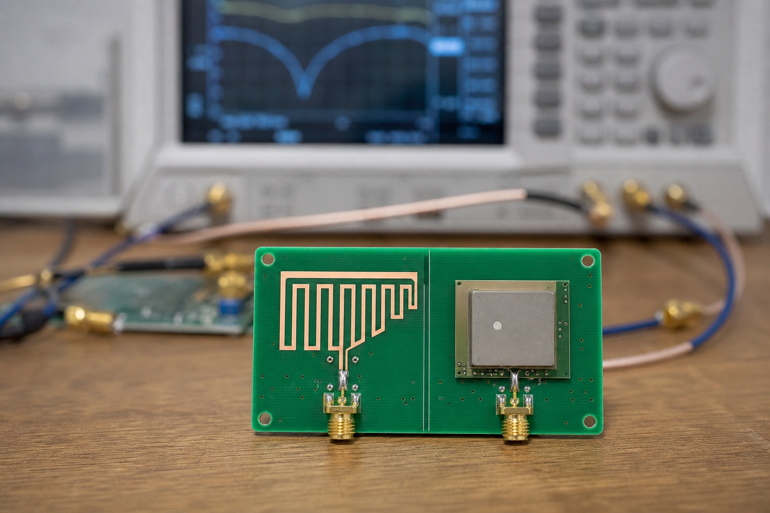
At 2.4 GHz on a compact IoT PCB, a well-executed PCB trace antenna (IFA or meander) performs within 1–2 dBi of a $0.15 chip antenna when the fab holds impedance tolerance and you respect keep-out. A chip antenna buys forgiveness on layout mistakes; a trace antenna buys BOM cost at the price of EM simulation time and fab sensitivity. We shipped both on the same product line (environmental sensor, nRF52840, BLE) and compared in an SV chamber and in field RSSI.
Candidates
| Antenna | Part / type | BOM | Matching network |
|---|---|---|---|
| Chip | Johanson 2450AT42E010BE | $0.15 @ 10k | 2-element PI, 0402 |
| PCB IFA | Custom 12×3 mm inverted-F | $0 | 3-element PI, tuned per board |
Stack-up: 4-layer, 1.6 mm, FR-4 Dk≈4.4, L1 RF feed, solid L2 ground, no components in 5 mm keep-out per Johanson app note (chip) and identical keep-out enforced for trace variant.
Simulation vs reality
- Sim: Keysight PathWave ADS with vendor substrate model for chip; trace antenna drawn from Nordic reference then adjusted in ADS Momentum
- Chamber: Satimo near-field, 2400–2483 MHz
- On-air: RSSI at 10 m LOS outdoor, 100 packets/s, nRF52840 +0 dBm
Results (peak gain, mid-band):
| Variant | Sim peak gain | Chamber peak | 10 m RSSI median |
|---|---|---|---|
| Chip + correct keep-out | 2.0 dBi | 1.8 dBi | -68 dBm |
| Chip, VIOLATED keep-out (cap too close) | — | 0.9 dBi | -74 dBm |
| PCB trace, 5 mil trace width | 1.6 dBi | 1.4 dBi | -70 dBm |
| PCB trace, fab ran 4.5 mil (out of tol) | — | 0.7 dBi | -78 dBm |
1–2 dB in chamber equals noticeable link margin at BLE sensitivity threshold.
Tradeoffs that mattered
Chip antenna
Pros: vendor characterization, less in-house EM expertise, smaller board area if vertical mount. Cons: placement rules sacred—one 0402 cap in keep-out cost 5 dB; height 2 mm affects slim enclosure.
PCB trace
Pros: no antenna line item, coplanar with ground easy on 4-layer. Cons: fab tolerance on trace width and dielectric constant shifts resonant frequency; every PCB spin may need matching tweak. Budget network analyzer time (NanoVNA V2 adequate for go/no-go, not for sign-off).
We added PI matching (Johanson 2450BM15A0018 matching chip on trace design for repeatability).
Layout rules we enforce in ERC
- No copper pour under antenna void except ground reference per design
- Feed via count minimized—one transition L1→L2 cost 0.3 dB in our A/B
- Crystal 32 MHz keep away 8 mm from RF feed (clock harmonics showed in EMI bench testing)
Protocol choice (BLE vs Thread) affects acceptable margin—see MQTT vs CoAP on CC2652 for gateway-side sensitivity to dropouts.
Certification note
Modular approval path favors certified chip modules (FCC ID on module). Custom trace on nRF52840 SoC requires intentional radiator filing on final product—legal/compliance cost, not RF physics. Chip on module (nRF52840-QIAA module variant) vs chip antenna on custom PCB is often a business decision more than 1 dBi.
What I'd do next
- Matching fixture in production test—reflectometer spot check VSWR < 2:1 at 2440 MHz, reject bad assemblies.
- Dual-source fab qualification—trace antenna designs validated per fab Dk measurement.
- Enclosure detuning study—plastic 0.8 mm above antenna shifted trace design 3 MHz; chip less sensitive in our sample of n=6.
Enclosure and human body detuning
Wearable prototype: hand proximity detuned PCB trace antenna −2 dB; chip antenna on ground plane extension less affected. Product marketing wanted smallest PCB—RF lost argument until field drop-rate data returned.
Anechoic vs office RSSI
Chamber gain within 0.5 dB repeatability; office RSSI varied 4 dB day-to-day (Wi-Fi congestion). Certify in chamber; validate in target environment with over-the-air packet loss metric, not RSSI alone.
Conducted vs radiated
Chamber results optimistic vs USB cable acting as radiator—FCC pre-scan showed USB 3.0 hub near DUT raised conducted emissions 3 dB on harmonic. Chip antenna benefit: smaller loop area, less cable coupling in cramped enclosure.
Second source antenna qualification
Johanson lead time spike forced Linx ANT-2.4-CHP alternative—required re-match PI network, one spin, $4k chamber time. Chip antenna modular approval easier to swap with pre-certified module than re-spinning custom trace.
Pre-certification sample size
FCC ID on module variant used 5 samples; custom trace design required 10 for variance on cheap fab. Budget chamber time in NPI schedule—trace antenna is not zero NRE.
Pick chip antenna when team lacks EM bench and enclosure is tight. Pick trace when BOM at 100k+ and you can own matching every spin. Neither works if keep-out is a suggestion.

Manish Bookreader
Electronics enthusiast, Embedded Systems Expert, Linux/Networking programmer, and Software Engineer passionate about AI, electronics, books, and cooking.