Power Sequencing Design Notes: When Rails Come Up in the Wrong Order
A processor that sees its I/O rails before its core rail will latch up. Hard to reproduce, catastrophic in production. A methodical approach to sequencing.
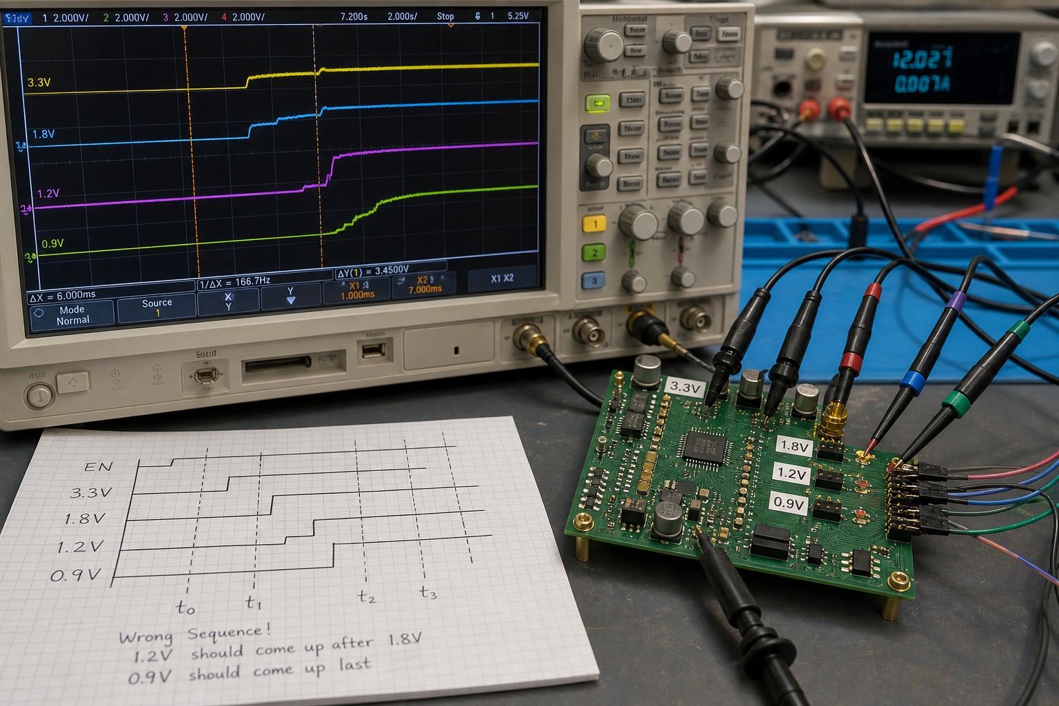
A processor that sees its I/O rails before its core rail will latch up. Hard to reproduce, catastrophic in production. A methodical approach to sequencing we adopted after one EVT lot showed 2% "no boot" that wasn't flash corruption.
Answer first
Define rail order, slew rate, and enable dependencies in the schematic review checklist before layout. Measure all rails relative to reset release with scope on same timebase — not one rail at a time. PMIC sequencing beats discrete POR hacks for anything with eMMC, SD, or USB-C PD front-end.
Incident setup
SoC: i.MX RT1064. Rails: VDD_SOC (1.1 V), VDD_HIGH_IN (3.3 V IO), NVCC_SD (3.3 V SD IO), USB_OTG (3.3 V). Sequencing PMIC: PCA9450 (NXP).
Symptom: 2% units never boot from SD; JTAG alive; ROM serial downloader OK. "Fixed" by power-cycle twice — classic sequencing marginality.
What went wrong
Reset released when 3.3 V IO was at 90% but 1.1 V core at 72% — within datasheet "typical" but below minimum at release spec we misread. eMMC first CMD line driven high into core still in POR — latch-up on IO buffer not catastrophic but SD controller entered zombie state until full power cycle.
Also: USB-C PD path enabled 5 V VBUS before PMIC finished core ramp on one schematic rev — OR-ing paths without blocking diode sequencing.
Measurement method
Four-channel scope:
| Ch | Probe |
|---|---|
| 1 | VDD_SOC |
| 2 | VDD_HIGH_IN |
| 3 | RESET_B (SoC) |
| 4 | SD_CLK (activity) |
Trigger: VDD_HIGH_IN crossing 3.0 V rising. Capture 50 ms. Overlay good vs. bad unit — bad showed RESET deassert 8 ms before VDD_SOC stable.
Use oscilloscope pulse/edge triggers on RESET falling edge with holdoff.
Sequencing design rules (our checklist)
1. Read SoC power-up chart literally
NXP/Freescale charts show order AND delay AND ramp monotonicity. "Typical 5 ms delay" isn't optional if min says 5 ms.
2. PMIC before discrete
PCA9450 / TPS65219 / MAX77654 — program order via OTP or I2C at manufacturing. Discrete RC delays drift with temperature and component tolerance.
We moved from RC-delay reset supervisor to PMIC PWRON sequencing — bad EVT units reworked.
3. Reset stays asserted until last critical rail OK
Use supervisor with mult rail monitor (MAX16056 class) or PMIC PGOOD AND gate — not single-rail 3.3 V supervisor alone.
4. Load switches on peripheral rails
SD, QSPI flash, RF PA — enable after core + IO valid. GPIO from SoC or PMIC LDO2 enable — document in devicetree regulator-init-microsecond.
5. Power-down order matters too
USB suspend → back-powering via IO — sequence down IO before core or use dedicated disable FETs.
Discrete fallback pattern (cost-sensitive)
When PMIC overkill (STM32G0 sensor node):
VIN → LDO core → (delay via supervisor PGOOD) → LDO IO → nRESET release
Delay from supervisor PGOOD, not GPIO bit-bang from booting MCU — chicken-and-egg.
USB-C + PMIC interaction
PD contract raises VBUS 9 V → buck ramps 3.3 V → LDO 1.8 V sensor — don't release sensor reset until 1.8 V within spec and PD PSSourceOn. Tied into PD state machine; see USB-C notes.
EMI testing caught one sequencing EMI issue: load switch enable edge coupled into analog front-end — solved with RC slew on enable, not faster sequencing.
Simulation
LTspice for RC POR — rough. iSim for PMIC models — better. Still verify on bench cold (-40 °C chamber) — capacitor ESR shifts delays; we saw boot fail only cold until PGOOD threshold adjusted.
Production test
ICT checks presence of sequencing components — not enough. Functional test:
- Slow ramp supply 0→5 V in 500 ms
- Fast plug USB-C (human or fixture)
- Brownout pulse 3.3 V dip 20 ms during boot
Log boot count in test firmware — fail if SD init fail bit set.
Three products summary
| Product | Sequencing solution | Failure mode prevented |
|---|---|---|
| RT1064 gateway | PCA9450 OTP seq | SD zombie boot |
| nRF52840 wearable | onboard LDO order fixed | no issue (simple rails) |
| ESP32-S3 puck | manual EN + USB OR | back-power via UART adapter |
What I'd do next
Standardize PMIC family per vendor to reuse sequencing playbooks — NXP for i.MX, TI for battery-heavy.
Add sequencing diagram page to every schematic PDF export — ops reviews photos, not source files.
Power sequencing isn't bring-up polish. It's defining when silicon is allowed to think — get it wrong and software looks broken forever.
PMIC programming gotcha (PCA9450)
OTP-programmed sequence on first power-up from NXP programmer — not the same as I2C runtime tweak. We changed runtime sequence in firmware thinking we fixed EVT; OTP sequence still ran first 100 ms at POR until we regenerated OTP image. Read "Power-Up Sequence Configuration" twice.
Supervisor selection table
| Part | Monitors | Release delay |
|---|---|---|
| TPS3890 | single rail | adjustable |
| MAX16056 | dual rail AND | fixed |
| PCA9450 PGOOD | multi-rail | integrated |
Using TPS3890 on 3.3 V only while core ramps separately — how we got 2% boot fail. Dual monitor or PMIC PGOOD.
What I'd do next

Manish Bookreader
Electronics enthusiast, Embedded Systems Expert, Linux/Networking programmer, and Software Engineer passionate about AI, electronics, books, and cooking.