Flash Write Endurance: Counting Cycles in Production Firmware
Writing to the same flash page on every sensor sample will kill the MCU before the product's warranty expires. Wear leveling strategies for internal flash.
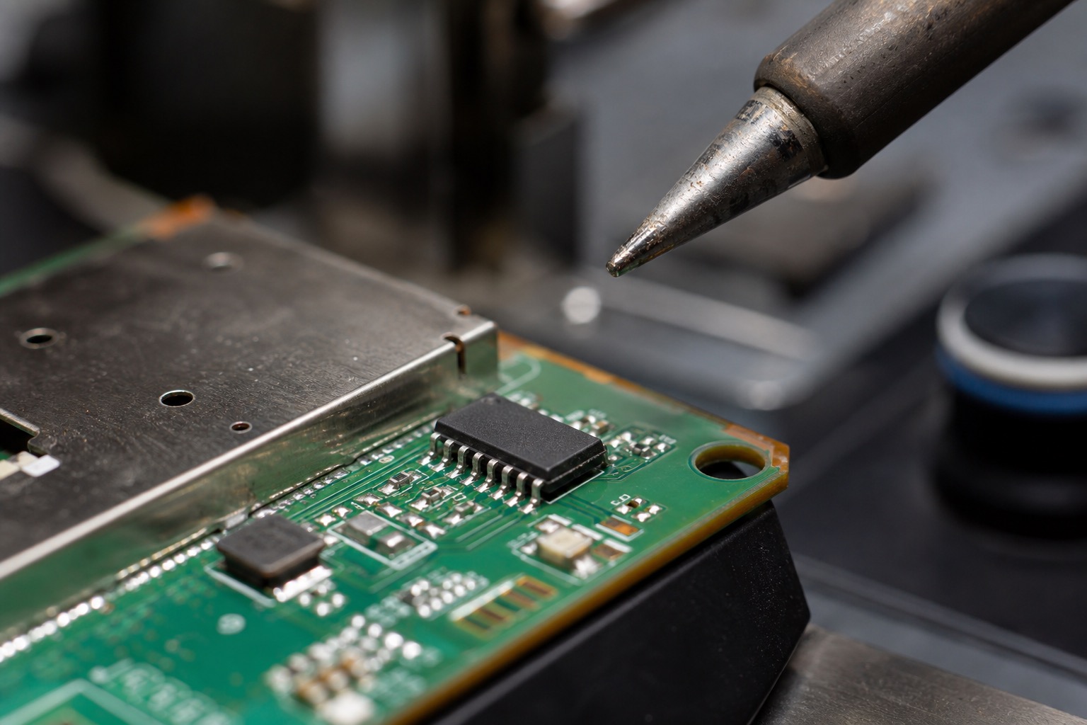
Writing sensor samples to the same flash page every 60 seconds will erase that page in weeks. STM32G0 internal flash endurance is 10k cycles typical — do the arithmetic before warranty expires. This note covers wear math, ring-buffer strategies in internal flash, and when to move to external EEPROM or FRAM.
Related: OTA update bootloader design, MCUboot integration notes.
The failure I almost shipped
Product spec: log temperature max/min every minute to internal flash for 10-year battery life.
Implementation draft:
typedef struct {
    int16_t t_min;
    int16_t t_max;
    uint32_t timestamp;
} sample_t;

void save_sample(sample_t s) {
    flash_erase_page(CONFIG_ADDR);
    flash_write(CONFIG_ADDR, &s, sizeof(s));
}
STM32G071: 2 KB page at end of flash, endurance 10k erase cycles.
Cycles per year: 525,600 minutes → 525,600 erases/year on one page.
Time to death: 10,000 / 525,600 ≈ 7 days.
QA caught it in review. Field would not.
Endurance numbers to look up (never assume)
| Part | Endurance (typical) | Page/sector size |
|---|---|---|
| STM32G0 | 10k cycles/page | 2 KB |
| STM32L4 | 10k | 2 KB |
| nRF52832 NVMC | 10k | 1 KB (older docs) |
| External AT24C256 EEPROM | 1M write cycles (byte) | N/A |
| FRAM CY15B104 | 10^12 cycles | N/A |
Always read your revision's reference manual errata — some lines specify 100k for certain batches marketing calls "enhanced."
Wear math template
cycles_to_failure = endurance / erases_per_year
erases_per_year = (samples_per_day × 365) / pages_in_rotation
If rotation uses 32 pages:
erases_per_page_per_year = (525600 / 32) ≈ 16425 → still exceeds 10k in year 1
Need either larger rotation set, less frequent commits, or external storage.
Strategy 1: Ring buffer with page-level rotation
Append-only log within page until full, then erase next page in ring.
Page 0: [rec][rec][rec]... full → erase Page 1, write pointer moves
...
Page N-1 full → erase Page 0 (oldest data lost if not uploaded)
Erases per year with 32 pages, 1 sample/min, one record per page fill assuming 32 records/page (~64 bytes each, 2KB page):
Records per page ≈ 32 Minutes per page erase ≈ 32 Erases per page per year ≈ 525600/32 ≈ 16425 — still too high.
Conclusion: minute-level logging to internal flash requires many pages OR batching many records per erase.
Batch 60 samples in RAM, one record write per hour:
Erases/hour = 1 / pages_in_ring
Per page per year = 8760 / pages_in_ring
With 16 pages: 547 erases/page/year → 10k endurance ≈ 18 years ✓
Strategy 2: RAM buffer + periodic commit
Hold 24 hours of samples in RAM (battery-backed or accept loss on reset). Commit once per day to flash ring.
Tradeoff: power loss loses up to 24 h data — product decision, not firmware alone.
Strategy 3: External storage
AT24C256 I2C EEPROM: 512 bytes/page, 1M cycle endurance per byte cell if you rotate addresses within page carefully — still wear-level byte addresses across 32k bytes.
MRAM/FRAM if BOM allows ($1–3): cycle count stops being the constraint; retention and power do.
For consumer qty >100k, external EEPROM often cheaper than support calls from dead flash.
Implementation sketch: flash ring on STM32 HAL
#define FLASH_PAGE_SIZE   2048
#define FLASH_PAGE_COUNT  16
#define FLASH_BASE_ADDR   0x0801F000  /* last 32KB */

typedef struct {
    uint32_t magic;
    uint32_t seq;
    sample_t data;
    uint32_t crc;
} flash_record_t;

static uint32_t write_idx;  /* persisted in RTC backup reg or first page header */

int flash_log_append(sample_t *s) {
    flash_record_t rec = { .magic = 0xA5A5, .seq = next_seq++, .data = *s };
    rec.crc = crc32(&rec, offsetof(flash_record_t, crc));

    uint32_t addr = FLASH_BASE_ADDR + (write_idx % (FLASH_PAGE_COUNT * FLASH_PAGE_SIZE));
    if ((addr % FLASH_PAGE_SIZE) == 0) {
        HAL_FLASHEx_Erase(&erase_init_for_page(addr));
    }
    HAL_FLASH_Program(..., addr, (uint64_t*)&rec, ...);
    write_idx += sizeof(rec);
    return 0;
}
Production code needs:
- Power-loss safe commit (write status flags, double-buffer)
- CRC on read
- Upload/drain path so ring does not fill permanently
Counting cycles in production firmware
Expose debug metric:
uint32_t flash_erase_count_total; /* increment on each erase */
Log to telemetry once per day. Alert if (erase_count / days_since_boot) > budget.
Factory test: do not run burn-in loops on production flash region — use dedicated test sector or RAM mock.
Interaction with OTA
MCUboot swap or overwrite moves erase traffic to different regions. Your log ring must not overlap bootloader slots or NVS partition.
Check generated .map and devicetree flash_partitions:
slot0_partition:  140 KB
slot1_partition:  140 KB
storage_partition: 32 KB  ← your ring lives here only
See OTA bootloader design and MCUboot integration.
NVS / settings subsystem
Zephyr settings + NVS backend wear-levels across sectors — use it instead of rolling your own if on Zephyr. Config:
CONFIG_NVS=y
CONFIG_SETTINGS=y
CONFIG_SETTINGS_NVS=y
Still bounded by partition size — monitor settings_nvs garbage collection erases.
What I would decide today
| Sample rate | Storage |
|---|---|
| Sub-second | RAM + batch, or no flash |
| Minutes | Hourly batch to 16+ page ring |
| Hours/days | Direct flash or EEPROM |
| 10-year cert | External FRAM or EEPROM |
Never erase-per-write on internal flash for recurring telemetry. That is the whole note.
Related
OTA bootloader design for partition layout. MCUboot integration for not stomping slots during logging.

Manish Bookreader
Electronics enthusiast, Embedded Systems Expert, Linux/Networking programmer, and Software Engineer passionate about AI, electronics, books, and cooking.