Thermal Camera PCB Debugging: Five Cases Where It Found What the DMM Missed
A $300 thermal camera paid for itself in the first week. Hotspots, bad solder joints, and a regulator running 40°C above its expected temperature.
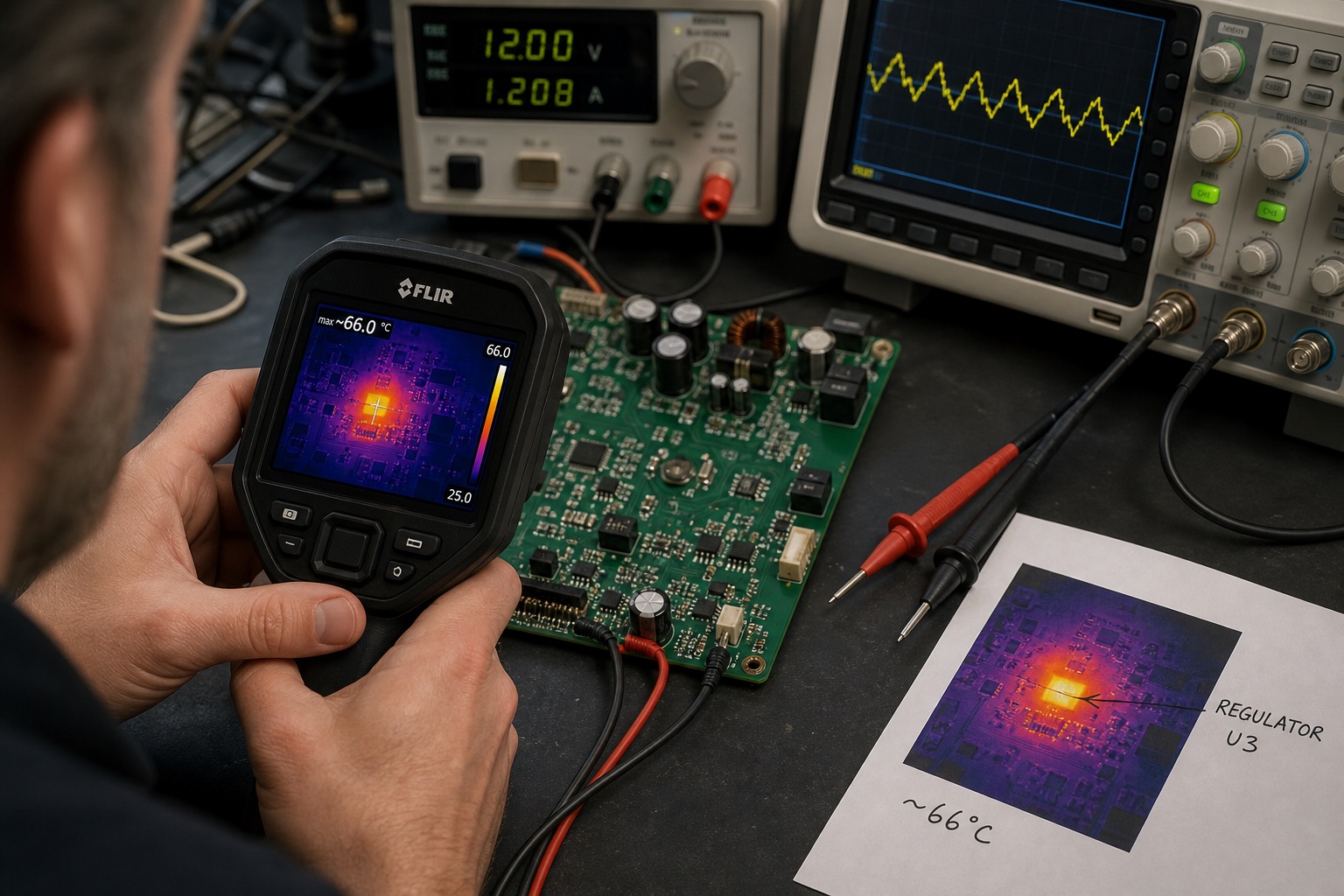
A FLIR C5 (160×120, 9 Hz, ~$299 street) paid for itself in the first week on our bench — not because it replaced a DMM, but because it shows power dissipation geography the DMM cannot. Five cases from 2024–2025 hardware bring-up where thermal imaging found the fault first.
Bench workflow integration
Our bring-up SOP step 4 is now thermal scan at 50% load, 100% load, and 5 minutes after power-down — compare to golden images stored in hardware/thermal-golden/. Delta-T > 15°C vs golden triggers EE review before ship.
FLIR MSX blending (visible + IR) helps correlate hotspot to ref des on dense boards — enable in export for incident attachments.
Safety and false confidence
Thermal cameras do not see through copper pour — hotspot under plane may be on opposite layer. Flip board or use narrow angle. Do not touch hot parts based on IR alone; confirm temperature with thermocouple on first occurrence of unknown hotspot class.
We keep a $40 K-type thermocouple on the bench for spot validation — thermal camera for discovery, thermocouple for sign-off on thermal limit violations.
Store thermal PNGs with board serial, load condition, and ambient temp in EXIF comment field — future you will forget which capture was which.
Case 1 — LDO running 40°C above ambient
Board: 3.3 V rail from MIC5504-3.3YM5 (SOT-23-5), expected loss ~150 mW at 150 mA load.
DMM: 3.28 V at output — "fine."
Thermal: package at 62°C in 22°C lab (40°C rise). Input was 5.0 V — design intended 3.7 V lithium. Extra 255 mW in LDO.
Fix: swap to buck TPS62740 or correct input source. DMM would eventually find wrong input if you thought to measure it; thermal pointed at the LDO itself as suspect in 10 seconds.
Case 2 — Bad QFN solder on thermal pad
STM32H743VI, 0.5 mm pitch QFN-100. DMM on 3.3 V rail: 3.31 V. Logic analyzer: intermittent SPI garbage.
Thermal: corner of MCU package 8°C hotter than opposite corner; center pad region cold — classic voided thermal pad.
Fix: reflow with proper paste volume on exposed pad stencil. X-ray later confirmed 40% void on bad unit.
Cross-tool: logic issues often need oscilloscope trigger discipline; thermal narrowed where to probe.
Case 3 — Reverse polarity protection P-FET half-on
Si2301CDS P-FET body diode protecting USB-C input. Normal load: DMM shows 4.95 V. Under 2 A load: 4.1 V — if you measure then.
Thermal: FET at 85°C at only 500 mA — operating in linear region. Gate pull-up resistor wrong value (47 k vs 4.7 k) — slow turn-on + insufficient Vgs.
Fix: schematic errata. Thermal spotted FET as hotspot before we loaded to 2 A.
Case 4 — Via-in-pad uncapped stealing heat from neighbor
DDR3 area: one via-in-pad on 0.8 mm pitch BGA power pin uncapped, solder wicking during reflow. DMM: net continuity OK. JTAG intermittent.
Thermal post-reflow: single pad consistently 3°C cooler — insufficient solder fillet.
Fix: cap vias on all power pads per fab rule 2.4. KiCad 7 DRC helps catch — see KiCad 7 workflow notes.
Case 5 — EMI-induced heating on ferrite bead
Not a failure — diagnostic. Bead on SDIO line hot at 55°C during Wi-Fi transmit test. DMM: negligible DC drop.
Near-field probe + thermal correlated common-mode energy on SDIO, not bead rating failure. Added CM choke; bead temp normalized.
Leads to formal EMI bench testing before chamber time.
Technique notes
Emissivity: FR4 ~0.95, aluminum electrolytic can ~0.85, shiny copper misleading — apply matte tape spot or adjust emissivity setting on C5.
Reflective surfaces: heat mirror from neighboring hot part — move angle, reduce reflected IR.
Resolution limit: 160×120 cannot resolve 0603 individually at 30 cm — move closer (min focus ~15 cm on C5).
Absolute vs relative: for bring-up, delta-T matters more than absolute temperature. Compare symmetric rails A vs B.
When DMM still wins
- Quiescent current in uA sleep — thermal noise floor
- Exact voltage reference validation
- Short location with milliohm bench setup
Use both. Order on our bench: visual → thermal scan → DMM on suspicious net → scope if switching.
Equipment
- Camera: FLIR C5, firmware 3.0.2
- Also tested Seek CompactPRO — narrower FOV, similar utility
- High-end: FLIR E54 ($$$) — only justified if weekly compliance thermal reports
What I'd do next
Document golden thermal images of known-good boards at defined load (50%, 100%) — diff on failure triage like comparing waveforms.
Integrate thermal photo attachment in hardware incident template — "hotspot screenshot" mandatory for power-related tickets.
Train team on inrush vs steady-state — capture video mode (9 Hz) during power-up; one-shot misses surge heating on bulk cap ESR.

Manish Bookreader
Electronics enthusiast, Embedded Systems Expert, Linux/Networking programmer, and Software Engineer passionate about AI, electronics, books, and cooking.