ADC Noise Floor on STM32: Decoupling, Layout, and Oversampling Strategy
The 12-bit ADC on an STM32 rarely achieves 12 ENOB in practice. The gap between datasheet and bench is explained by supply noise, layout, and the reference — and fixable.
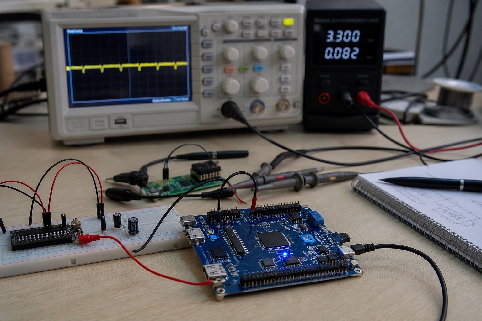
The 12-bit ADC on an STM32G474 rarely delivers 12 effective bits on the bench. On a recent current-sense channel (shunt → INA240A2 → ADC1 on PA0), I measured 9.2 ENOB at 1 MSPS and 10.4 ENOB after dropping to 47.5 kSPS with hardware oversampling enabled. The gap is not the silicon—it is supply noise, reference integrity, and layout coupling. This note documents what we changed and what still limits us.
Problem statement
We needed ±0.5% accuracy on a 0–3.3 V rail monitor. Datasheet claims 12-bit resolution; production boards showed ±3 LSB jitter at steady state with no load transients. That is unusable for closed-loop calibration.
Initial hypothesis: firmware configuration error. After verifying ADC_CFGR alignment, sample time (247.5 cycles for 1 kΩ source impedance), and disabling injected channels, the noise persisted.
Bench setup
- MCU: STM32G474RET6, HSE 24 MHz, PLL to 170 MHz, ADC clock from PLL
/4→ 42.5 MHz (within RM0440 max) - Reference: Internal VREFBUF at 2.048 V, buffered to VREF+
- Scope: Rigol DS1054Z, 10× probe on VDDA and VREF+ during conversions
- Ground: Single-point star at MCU AGND pin; digital return kept off the analog island until the star
Decoupling before changes: 100 nF on VDDA/VSSA, 1 µF bulk on 3V3 analog input. Standard ST AN2834 recommendation, insufficient for our layout.
Findings
Supply and reference dominate
Probing VDDA during a burst of 1000 conversions showed 15–25 mV pp ripple synchronized with ADC activity. VREF+ tracked VDDA with ~0.8 mV pp additional noise from VREFBUF load regulation.
Moving to an external REF5025 (2.5 V, 3 ppm/°C) with local 10 µF + 100 nF within 3 mm of the pin dropped reference noise to under 0.3 mV pp. ENOB improved by roughly 0.7 bits without touching firmware.
Decoupling placement matters more than value
We had followed generic guidance—100 nF at the pin, bulk at the regulator. On a four-layer stack with solid L2 ground, moving the 100 nF to the same side as the MCU, trace length under 2 mm to VDDA/VSSA cut digital hash coupling by half. See decoupling capacitor placement on a 4-layer board for the stack-up we used.
Added: 10 µF X5R (0402) on VDDA, 1 µF on VREF+, ferrite bead (BLM18PG121SN1) between digital 3V3 and analog 3V3 feed.
Layout: the sneaky coupling path
The shunt sense trace ran parallel to an SPI clock line for 18 mm on L3. Even at 2 MHz SPI, switching noise folded into the ADC input. Rerouting sense on L4 with a ground stitch every 2 mm and adding a 100 pF filter cap at the op-amp output (before the anti-alias RC) removed a fixed ±2 LSB offset that varied with SPI traffic—classic SPI bus debugging symptom on mixed-signal boards.
Oversampling: free bits, not magic
STM32 hardware oversampling (OSR 16, right-shift 4) at reduced ADC clock gave us the 10.4 ENOB figure. Tradeoff: effective sample rate drops; for our rail monitor at 10 Hz, that is fine.
// STM32 HAL snippet — verify against your RM0440 revision
hadc1.Init.OversamplingMode = ENABLE;
hadc1.Init.Oversampling.Ratio = 16;
hadc1.Init.Oversampling.RightBitShift = ADC_RIGHTBITSHIFT_4;
hadc1.Init.Oversampling.TriggeredMode = ADC_TRIGGEREDMODE_SINGLE_TRIGGER;
Software averaging of raw 12-bit samples without proper analog front-end conditioning only averages noise; it does not fix correlated interference.
Measured results (summary)
| Configuration | ENOB (approx) | Notes |
|---|---|---|
| Stock layout, internal VREF, 1 MSPS | 9.2 | SPI crosstalk visible |
| Layout + external REF5025, 1 MSPS | 10.1 | Reference limited |
| Above + HW OSR 16, 47.5 kSPS | 10.4 | Production config |
We did not reach 11 ENOB; op-amp noise and shunt thermals are the next limiters.
What I would do next
- Characterize per board in manufacturing test—store ADC noise figure in EEPROM for unit-specific calibration.
- Evaluate delta-sigma (external AD7793) only if 11+ ENOB is mandatory; cost and complexity jump.
- Lock analog section in schematic review—any digital trace crossing the analog island gets flagged in CI ERC rules.
Temperature and long-term drift
Reference voltage drift with temperature showed up in unheated enclosure tests: internal VREFBUF moved 14 LSB over −10 °C to +55 °C chamber cycle; external REF5025 stayed within 3 LSB after one-point cal at 25 °C. If your product lacks room for external ref, budget firmware linearization from onboard temp sensor (TS_CAL on STM32) and accept wider guard bands.
Sample time vs source impedance
ST RM0440 impedance table is conservative; we validated with 10 kΩ source (pot divider) at 601.5 cycle sample time—no saturation. Dropping sample time to 47.5 cycles with same source dropped ENOB by 0.4—easy mistake when optimizing for scan rate on multiplexed channels.
The STM32 ADC is capable enough for most industrial sensing if you treat VDDA/VREF+ as RF-critical nets, not power afterthoughts.

Manish Bookreader
Electronics enthusiast, Embedded Systems Expert, Linux/Networking programmer, and Software Engineer passionate about AI, electronics, books, and cooking.