SWD vs JTAG: When the Choice Actually Matters
SWD uses two wires vs JTAG's four and works fine for single-core flashing and debugging. The cases where JTAG's daisy-chain and boundary scan capabilities are worth the extra pins.
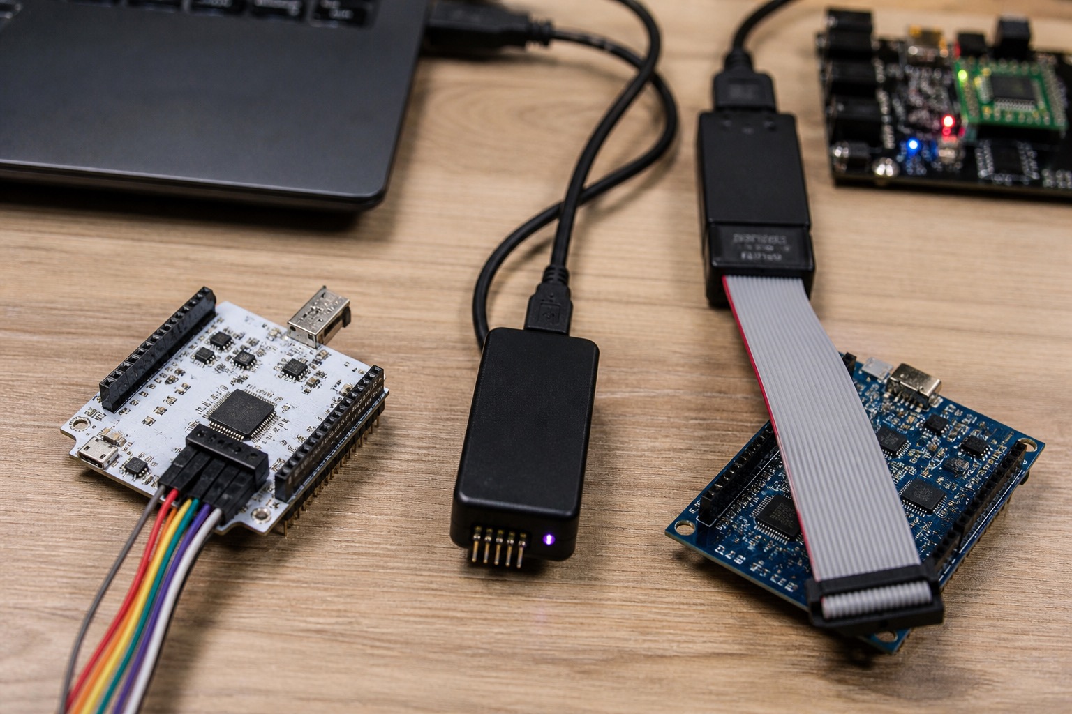
SWD (Serial Wire Debug) uses two data pins—SWDIO and SWCLK—plus ground and optional reset. JTAG uses four mandatory signals—TDI, TDO, TMS, TCK—and supports daisy-chained devices and boundary scan. For single-core Cortex-M bring-up, SWD is the default: fewer pins, same flash/debug you need. JTAG earns its pins when you chain MCUs, need IEEE 1149.1 boundary scan, or debug heterogeneous tap controllers.
SWD in daily use
- Pins: SWDIO, SWCLK, GND, nRESET (recommended), VTref sense
- Protocol: ARM ADIv5, packetized AP/DP access
- Typical tools: ST-Link, BMP, J-Link (SWD mode), OpenOCD
transport select swd
On STM32F407 bring-up, SWD at 4 MHz SWCLK stable with 15 cm cable—adequate for flash programming under 10 s for 512 KB.
# OpenOCD SWD — STM32F4
openocd -f interface/stlink.cfg -f target/stm32f4x.cfg
# default transport is swd on recent configs
Limitations:
- One debug port per connector (no native multi-tap daisy chain)
- No boundary scan for bed-of-nails structural test
- Some vendor secure MCUs restrict SWD after fuse—JTAG may also be restricted identically
JTAG when it matters
Daisy-chained MCUs
Product: main STM32H7 + coprocessor ESP32 (JTAG) + CPLD on one header. JTAG chain order documented in schematic: TDI → CPLD → ESP → H7 → TDO.
OpenOCD cfg fragment:
jtag newtap stm32 cpu -irlen 4 -expected-id 0x6ba00477
jtag newtap esp32 cpu -irlen 5 -expected-id 0x120034e5
target create stm32h7x.cpu cortex_m -chain-position stm32.cpu
SWD cannot express this; separate SWD headers cost BOM and technician confusion.
Boundary scan (ICT)
Contract manufacturer wanted JTAG structural test on nets to SDRAM—SWD does not expose 1149.1 EXTEST. Added Tag-Connect TC2050-ARM2010 footprint, dual-mode strapping resistor: SWD default, JTAG for factory.
Multi-core complex SoCs
i.MX RT1170 dual-core: debug architecture uses SWD multiplexing but tooling often expects specific connect sequences—read NXP doc before assuming "just plug ST-Link."
Our OpenOCD + Black Magic Probe note covers practical GDB sessions; probe choice independent of SWD vs JTAG transport.
Pin budget comparison
| Interface | Signals (min) | Use case |
|---|---|---|
| SWD | 2 + GND | ARM single-target |
| JTAG ARM | 4 + GND | Chain, boundary scan |
| cJTAG (2-wire) | 1 data + clock | MSP430, some TI — not ARM SWD |
On 0201-heavy wearable, we saved 2 pins with SWD-only—those pins became charger status LEDs worth more than JTAG chain.
Signal integrity
Both fail similarly on bad layouts—long unterminated fly wires, SWDIO routed near switching regulator. Oscilloscope trigger cheat sheet helped catch SWCLK ringing when series resistor missing (22 Ω recommended near host/debugger).
Decision matrix
| Question | If yes → |
|---|---|
| Single Cortex-M only? | SWD |
| Multiple tap devices one header? | JTAG |
| Factory ICT boundary scan? | JTAG |
| Space-critical 6-pin header? | SWD |
| ARM SecurCore fuse locked? | Neither helps—you planned wrong |
Adapter folklore
ST-Link V2 clones report SWD fine until hot-plug across voltage domains—always common ground first. J-Link Base auto-detects SWD/JTAG on same connector if pinout strapped correctly.
What I'd do next
- Schematic symbol field
DEBUG=SWD|JTAG|DUALon every MCU sheet—layout opens wrong footprint otherwise. - Production program: SWD in field, JTAG chain test only at CM—do not expose JTAG header to customer unless threat model allows.
- Document IR lengths in OpenOCD config repo alongside board revision.
SWD frequency tradeoff
Higher SWCLK speeds flash faster until cable capacitance wins—4 MHz reliable on 15 cm, 8 MHz failed on 30 cm unshielded flat cable. OpenOCD adapter speed 4000 in CI; engineers use adaptive clocking on J-Link.
Debug in low-power modes
STM32 stop mode kills SWD unless DBGMCU_CR debug bits set during development—production fuse clears them. Missing sleep-debug config looks like "debugger connects but CPU frozen" for hours until you read RM debug chapter during bring-up.
SWD on ARMv8-M TrustZone
Secure/non-secure debug access split—connecting debugger without SAU configured looks like "cannot read memory" at 0x08000000. Config script in OpenOCD must match TZ enable state; JTAG same pain, more forum posts.
Tag-Connect vs full header
Production uses Tag-Connect TC2050 footprint—SWD only, saves board space. Technicians hate it until they have pogo fixture; reliability at CM equals 2.54 mm header once fixture amortized over 10k units.
Adapter firmware updates
ST-Link V2J37 vs clone V2J15 behave differently on SWD connect under reset—document probe firmware in CI log header. Debug "works on my laptop" often traces to probe revision diff, not code.
Combined SWD+UART debug header
We standardized 6-pin header: SWDIO, SWCLK, GND, TX, RX, 3V3—one cable for printf and debug. JTAG not routed on consumer boards; factory fixture pogo same header with strap to JTAG adapter for ICT only.
For ARM firmware engineers, SWD is the right default. Order JTAG pins when the factory or the second chip on the board demands it—not because the header looks professional with more wires.

Manish Bookreader
Electronics enthusiast, Embedded Systems Expert, Linux/Networking programmer, and Software Engineer passionate about AI, electronics, books, and cooking.